Reverse Engineering (RE) of Printed Circuit Board to Detect Patent Infringement

Reverse engineering (RE) is a valuable practice that involves the disassembly/teardown of a product to understand its components, design, and functionality. The process is applicable to technology, software, printed circuit boards (PCBS), and various other domains.

When it comes to intellectual property law, reverse engineering serves a significant role in detecting patent infringement and protecting IR rights. A product is disassembled to assess whether it contains patented technologies, processes, or designs. Further, reverse engineering allows businesses to ensure their product does not infringe on existing rights while still maintaining a competitive edge.

In this article, we’ll explore how reverse engineering of PCBs help to detect patent infringement and the steps involved in this process. We’ll provide a clear overview of how this technique uncovers potential IP violations and protects innovation in the tech industry.

Need of Reverse Engineering (RE) in Printed Circuit Board (PCB)

With the growing popularity of electronic devices such as smartphones, smart TVs, tablets, and AR/VR systems, opportunities for monetization through licensing and royalties have significantly increased. However, this market expansion also heightens the risk of unauthorized use or duplication of patented technologies.

Printed circuit boards (PCBs) are one of the key components in electronic devices and often contain critical elements of patented innovations. For this very reason, reverse engineering is applied to closely examine the PCB’s design, materials, and layout to uncover patent infringements that might otherwise remain undetected.

Therefore, PCB reverse engineering plays a vital role in safeguarding innovation, enforcing patent rights, and maintaining compliance within the rapidly evolving electronics industry. Let’s explore how reverse engineering a printed circuit board can provide evidence of potential patent infringement.

Proving Patent Infringement in Printed Circuit Boards with Reverse Engineering

In printed circuit boards, where much of the infringement may not be externally visible, reverse engineering is often essential to uncover hidden features, collect evidence, and validate IP claims. This process involves a detailed examination of the PCB’s functional characteristics, physical layout, materials, and manufacturing techniques.

Through such analysis, intellectual property (IP) experts can assess whether the internal structure or operation of the accused PCB replicates a patented design or method.

In the following sections, we will outline a step-by-step approach to reverse engineering a printed circuit board for identifying potential patent infringement.

How to Conduct Reverse Engineering in Printed Circuit Boards (PCB)?

Step 1: Initial Visual Inspection and Datasheet Review

The process begins with a careful visual inspection of the printed circuit board (PCB). This step involves identifying and documenting the various components such as resistors, capacitors, connectors, and integrated circuits (ICs) as well as noting their physical arrangement and any labelling or part numbers.

We take high-resolution photographs for reference and analyse component datasheets to verify the parts’ specifications and intended functions. This initial inspection provides critical baseline information about the PCB’s architecture, potential signal pathways, and design intent. It also helps us assess the complexity of the circuit, understand the likely function of each section of the board, and plan the subsequent steps in the reverse engineering process more effectively.

Reverse Engineering in Printed Circuit Boards (PCB)

Source


Step 2: Component Identification and Extraction

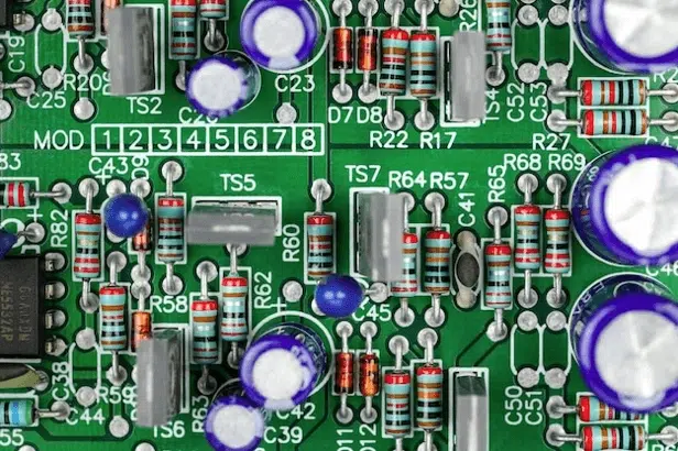
In some cases, surface-mounted or through-hole components may obscure the underlying traces, vias, or pads, making it difficult to fully analyze the PCB’s electrical pathways. When necessary, we proceed with the careful removal of components to expose the hidden layers and interconnections beneath them.


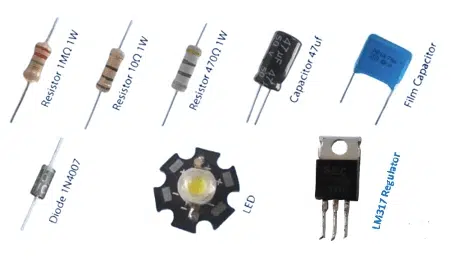
This step must be done with precision to avoid damaging the PCB or its conductive layers. We use specialized tools such as a heat gun and a desoldering station to safely detach components while preserving the integrity of the parts and the board. During this process, key information such as component type, part number, and their precise location on the board is meticulously documented for further analysis.

Component Identification and Extraction

Source

Step 3: Circuit Tracing and Schematic Mapping

The next critical step in reverse engineering a PCB is tracing the connections between the various components. Using a multi-meter in continuity mode, we manually trace each connection on the board to ensure we understand how the components are electrically linked. This process often involves checking pin-to-pin continuity to confirm the paths between specific points on the circuit, which helps us accurately map the electrical layout of the board.

Circuit Tracing and Schematic Mapping

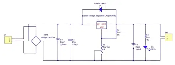
To document the connections, we either sketch them manually on graph paper or utilize digital software to create a more precise and organized representation of the circuit. Digital tools are useful for larger or more complex PCBs, where visualizing the connections and the relationships between components becomes critical. Additionally, software-based tracing tools allow us to identify and map the traces more efficiently, creating digital schematics that can be easily analyzed and compared against the original patent design.

Initial Visual Inspection and Datasheet Review


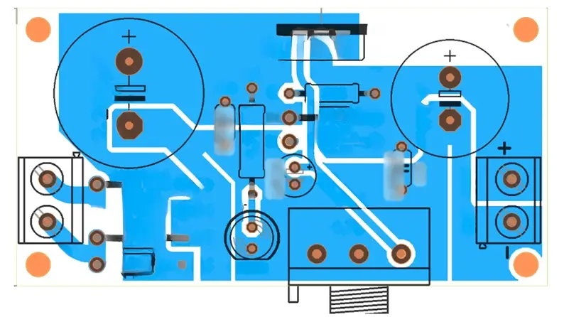
This step provides a comprehensive map of the circuit’s functionality and is essential for identifying design similarities, uncovering potential patent violations, and ensuring that we have an accurate understanding of the board’s electrical behavior.

Map of the circuitΓÇÖs functionality

Component Identification and Extraction

Step 4: Signal Path Analysis and Functionality Verification

After mapping the physical connections on the PCB, we analyze how signals travel through the circuit. While tracing paths with a multi-meter provides the static electrical layout, understanding the dynamic behavior of those signals is equally critical. Using tools such as oscilloscopes, logic analyzers, and advanced signal integrity software like Sigrity X, we examine signal quality, timing, interference, and overall performance across the PCB.

Eye diagram showing current Signal flow analysis

Eye diagram showing current Signal flow analysis

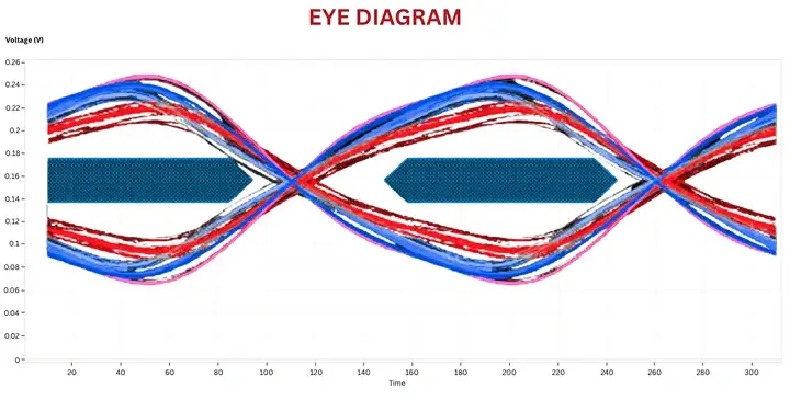
This step includes key analyses such as generating eye diagrams to visualize signal clarity and timing accuracy, conducting impedance analysis to check for transmission line mismatches, and assessing power ripple to identify any fluctuations that may affect sensitive components. These evaluations provide insight into real-world performance, revealing issues that may not be evident from a physical trace alone.

eye diagram

impedence analysis

Power Ripple Analysis

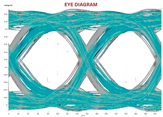
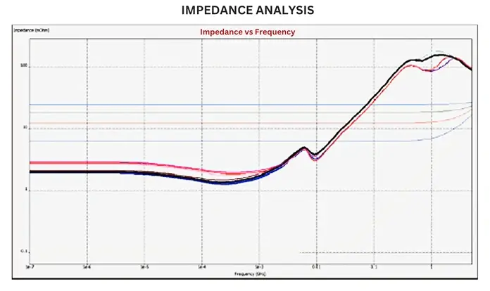
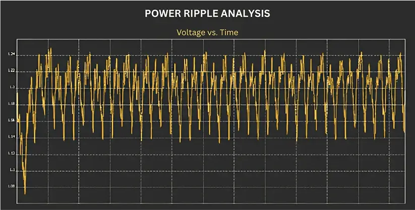
All findings are carefully documented with corresponding images, waveforms, and technical notes, building a comprehensive picture of how the circuit operates under actual conditions. Whether the goal is to detect patent infringement, troubleshoot design flaws, or study a competitor’s product, signal path analysis ensures a deep functional understanding of the PCB’s electronic behavior.

Step 5: Material Analysis

To determine the materials used in a Printed Circuit Board (PCB), several methods can be employed, each providing insights into the composition and structure of the board. The most straightforward approach is to analyze the PCB design files, which are typically created using Computer-Aided Design (CAD) software. These files contain detailed information about the materials specified for the PCB, including the types of substrates, conductive traces, and any additional components. By reviewing these files, one can identify the primary materials used, such as the substrate (often FR-4, a fiberglass-reinforced epoxy laminate) and the conductive traces.

Examining the physical board itself is another effective method. The most common material for traces on a PCB is copper due to its excellent electrical conductivity and cost-effectiveness. However, in specialized applications, other materials may be used. For instance, aluminum is sometimes employed in high-frequency applications, while silver and gold may be used for their superior conductivity and resistance to corrosion, albeit at a higher cost. Visual inspection can reveal the color and texture of the traces, which can provide clues about the materials used.

For more detailed analysis, especially when the composition is not readily apparent, advanced techniques can be utilized. One such method is the use of an electron microscope, particularly a scanning electron microscope (SEM). SEM allows for high-resolution imaging of the PCB surface, enabling the identification of materials at the micro and nanoscale. This technique is particularly useful for examining the quality of solder joints, trace widths, and other critical features of the PCB.

How We Can Help?

We specialize in thoroughly applying Reverse Engineering (RE) techniques to Printed Circuit Boards (PCBs) to identify potential patent infringements. With a deep understanding of PCB design and manufacturing processes, we meticulously analyze the underlying components, materials, and construction methods to uncover any violations of intellectual property (IP) rights.

We can prepare a comprehensive claim chart or Evidence of Use (EOU) to clearly demonstrate how a patented technology is being implemented in your case. By providing you with precise documentation, we strengthen your position in legal proceedings and help protect your innovation from unauthorized use.

Get in touch with our subject matter experts today to ensure a robust analysis and reliable support for your PCB-related IP needs.

Get Quotes